 |
Fig.1 CVD preparation of high-quality graphene/h-BN planar heterojunction

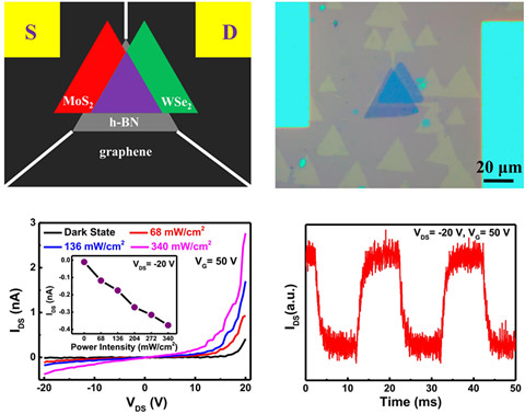
Fig. 2 Application of WSe2/MoS2 optoelectronic devices on Graphene/h-BN planar heterojunction
The Chinese Academy of Sciences Shanghai Institute of Microsystems and Information Technology has made new progress in the study of graphene/hexagonal boron nitride planar heterojunction. Researcher Xie Xiaoming’s research team has successfully prepared single atomic layer high quality graphene using chemical vapor deposition (CVD) method. Hexagonal Boron Nitride Planar Heterojunction and Successful Application to WSe2/MoS2 Two-dimensional Photodetector Devices The research paper Synthesis of High-Quality Graphene and Hexagonal Boron Nitride Monolayer In-Plane Heterostructure on Cu–Ni Alloy was published on Advanced Science on May 19th.
Graphene is similar to hexagonal boron nitride (h-BN) but has different electrical properties. As the graphene/hexagonal boron nitride planar heterojunction has important potential in basic research and device exploration, it has attracted much attention in the academic community. The graphene/h-BN planar heterojunction is generally prepared by sequentially depositing graphene and h-BN, or in reverse order, due to the difficulty of controlling the subsequent nucleation of the thin film and the fact that the reactive gas easily destroys the precursor film during growth. Therefore, the quality of the graphene/h-BN plane heterojunction is reported to be unsatisfactory at present. Lu Guangyuan and Wu Tianru of the State Key Laboratory of Functional Materials for Information Technology, Shanghai Institute of Microsystems based on the research basis for the growth of high-quality h-BN and graphene films on copper-nickel alloy substrates by first depositing h-BN single crystals and growing graphene, A high-quality graphene/h-BN planar heterojunction was successfully prepared. Since the growth rate of graphene on the copper-nickel alloy is extremely fast, the shorter deposition time of the graphene reduces the damage to the h-BN film during the growth of the graphene film. At the same time, due to the excellent catalytic ability of copper-nickel alloys, the random nucleation of graphene is eliminated while improving the crystal quality of the single crystal of boron nitride, making the graphene domains only in the vertices of triangular-shaped h-BN single crystal domains. Nuclei grow along the h-BN edge orientation. The research team cooperated with the team of Professor Jun Lou of the Rice University in the United States and used the cooperative training program of the doctoral student to use graphene as the contact electrode and h-BN as the insulation on the basis of the high-quality graphene/h-BN plane heterojunction. A WSe2/MoS2 two-dimensional photodetector was fabricated on the substrate, which verifies the quality and electrical properties of the graphene/h-BN planar heterojunction, and provides basic research and two-dimensional logic integrated circuit applications based on the heterojunction material platform. Exploration provides the foundation.
This work was supported by the major special project of the Ministry of Science and Technology “Wub-scale graphene electronic materials and devices research†and related research projects of the Chinese Academy of Sciences and the Shanghai Science and Technology Commission.
Glass Connecting System, Sliding Door System Hardware Manufacturers in China
Glass Sliding Door With Connector,Glass Sliding Door System,Glass Sliding Door System Connect,Swing Door Systemseries Glass Connecting
China Glass Sliding Door With Connector,Glass Sliding Door System,Glass Sliding Door System Connect,Swing Door Systemseries Glass Connecting, Most are available in Chrome, Brass, Brushed Stainless, Satin Chrome, and Gun Metal finishes we offered that you can trust. Welcome to do business with us.


Glass Sliding Door With Connector,Glass Sliding Door System,Glass Sliding Door System Connect,Swing Door Systemseries Glass Connecting
Leader Hardware Manufacturer Limited , https://www.leaderhardwarecn.com